


Addition is harder than you’d expect, at least for a computer.
Computers use multiple types of adder circuits with different tradeoffs of size versus speed.
In this article, I reverse-engineer an 8-bit adder in the Pentium’s floating point unit.
This adder turns out to be a carry-lookahead adder,
in particular, a type known as “Kogge-Stone.”1
In this article, I’ll explain how a carry-lookahead adder works and I’ll show how the Pentium implemented it.
Warning: lots of Boolean logic ahead.
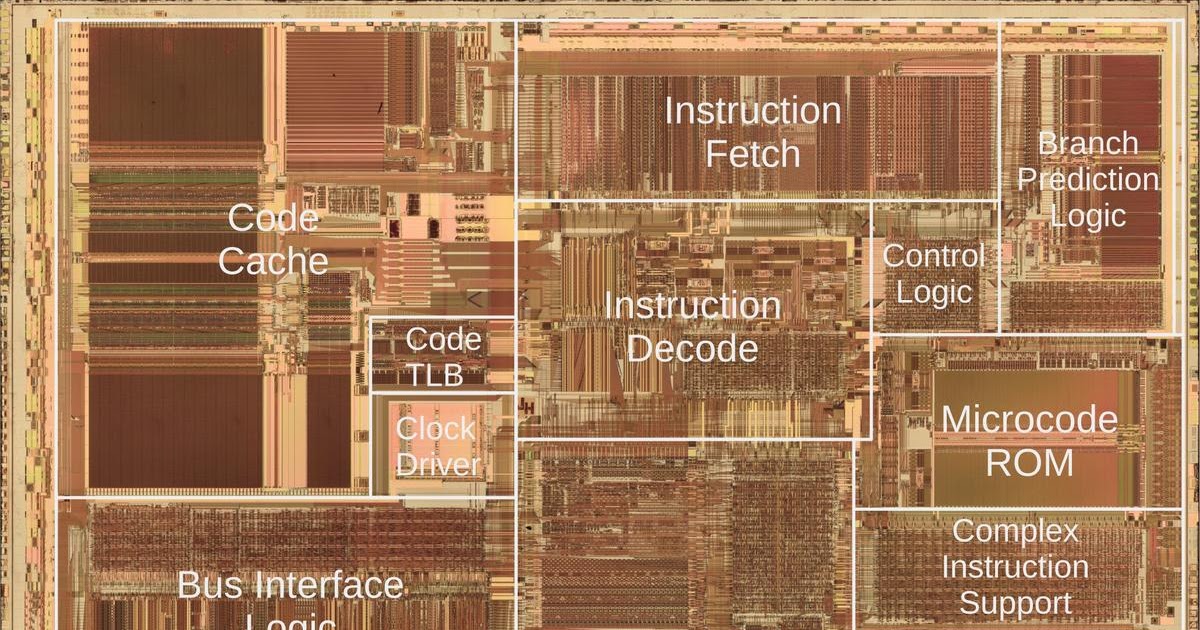
The Pentium die, showing the adder. Click this image (or any other) for a larger version.
The die photo above shows the main functional units of the Pentium.
The adder, in the lower right, is a small component of the floating point unit.
It is not a general-purpose adder, but is used only for determining quotient digits during division.
It played a role in the famous
Pentium FDIV division bug, which I wrote about here.
The hardware implementation
The photo below shows the carry-lookahead adder used by the divider.
The adder itself consists of the circuitry highlighted in red.
At the top, logic gates compute signals in parallel for each of the 8 pairs of inputs: partial sum, carry generate, and carry propagate.
Next, the complex carry-lookahead logic determines in parallel if there will be a carry at each position.
Finally, XOR gates apply the carry to each bit.
Note that the sum/generate/propagate circuitry consists of 8 repeated blocks, and the same with the carry XOR
circuitry.
The carry lookahead circuitry, however, doesn’t have any visible structure since it is different for each bit.2
The carry-lookahead adder that feeds the lookup table. This block of circuitry is just above the PLA on the die. I removed the metal layers, so this photo shows the doped silicon (dark) and the polysilicon (faint gray).
The large amount of circuitry in the middle is used for testing; see the footnote.3
At the bottom, the drivers amplify control signals for various parts of the circuit.
The carry-lookahead adder concept
The problem with addition is that carries make addition slow.
Consider calculating 99999+1 by hand.
You’ll start with 9+1=10, then carry the one, generating another carry, which generates another carry, and so forth, until you go through all the digits.
Computer addition has the same problem:
If you’re adding two numbers, the low-order bits can generate a carry that then propagates through all the bits.
An adder that works this way—known as a ripple carry adder—will be slow because the carry has to ripple through
all the bits.
As a result, CPUs use special circuits to make addition faster.
One solution is the carry-lookahead adder. In this adder, all the carry bits are computed in parallel, before computing
the sums. Then, the sum bits can be computed in parallel, using the carry bits.
As a result, the addition can be completed quickly, without waiting for the carries to ripple through
the entire sum.
It may seem impossible to compute the carries without computing the sum first, but there’s a way to do it.
For each bit position, you determine signals called “carry generate” and “carry propagate”.
These signals can then be used to determine all the carries in parallel.
The generate signal indicates that the position generates a carry. For instance, if you add binary
1xx and 1xx (where x is an arbitrary bit), a carry will be generated from the top bit,
regardless of the unspecified bits.
On the other hand, adding 0xx and 0xx will never produce a carry.
Thus, the generate signal is produced for the first case but not the second.
But what about 1xx plus 0xx? We might get a carry, for instance, 111+001, but we might not get a carry,
for instance, 101+001. In this “maybe” case, we set the carry propagate signal, indicating that a carry into the
position will get propagated out of the position. For example, if there is a carry out of
the middle position, 1xx+0xx will have a carry from the top bit. But if there is no carry out of the middle position, then
there will not be a carry from the top bit. In other words, the propagate signal indicates that a carry into the top bit will be propagated out of the top
bit.
To summarize, adding 1+1 will generate a carry. Adding 0+1 or 1+0 will propagate a
carry.
Thus, the generate signal is formed at each position by Gn = An·Bn, where A and B are the inputs.
The propagate signal is Pn = An+Bn,
the logical-OR of the inputs.4
Now that the propagate and generate signals are defined, they can be used to compute the carry Cn at
each bit position:
C1 = G0: a carry into bit 1 occurs if a carry is generated from bit 0.
C2 = G1 + G0P1: A carry into bit 2 occur if bit 1 generates a carry or bit 1 propagates a carry from bit 0.
C3 = G2 + G1P2 + G0P1P2: A carry into bit 3 occurs if bit 2 generates a carry, or bit 2 propagates a carry generated from bit 1, or bits 2 and 1 propagate a carry generated from bit 0.
C4 = G3 + G2P3 + G1P2P3 + G0P1P2P3: A carry into bit 4 occurs if a carry is generated from bit 3, 2, 1, or 0 along with the necessary propagate signals.
… and so forth, getting more complicated with each bit …
The important thing about these equations is that they can be computed in parallel, without waiting for a
carry to ripple through each position.
Once each carry is computed, the sum bits can be computed in parallel: Sn = An ⊕ Bn ⊕ Cn. In other words, the two input bits and the computed carry are combined with exclusive-or.
Implementing carry lookahead with a parallel prefix adder
The straightforward way to implement carry lookahead is to directly implement the equations above.
However, this approach requires a lot of circuitry due to the complicated equations.
Moreover, it needs gates with many inputs, which are slow for electrical reasons.5
The Pentium’s adder implements the carry lookahead in a different way, called the “parallel prefix adder.”7
The idea is to produce the propagate and generate signals across ranges of bits, not just single bits as before.
For instance, the propagate signal P32 indicates that a carry in to bit 2 would be propagated out of bit 3.
And G30 indicates that bits 3 to 0 generate a carry out of bit 3.
Using some mathematical tricks,6 you can take the P and G values for two smaller ranges and merge them into
the P and G values for the combined range.
For instance, you can start with the P and G values for bits 0 and 1, and produce P10 and G10.
These could be merged with P32 and G32 to produce P30 and G30,
indicating if a carry is propagated across bits 3-0 or generated by bits 3-0.
Note that Gn0 is the carry-lookahead value we need for bit n, so producing these G values gives
the results that we need from the carry-lookahead implementation.
This merging process is more efficient than the “brute force” implementation of the carry-lookahead logic since
logic subexpressions can be reused.
This merging process can be implemented in many ways, including
Kogge-Stone, Brent-Kung, and Ladner-Fischer.
The different algorithms have different tradeoffs of performance versus circuit area.
In the next section, I’ll show how the Pentium implements the Kogge-Stone algorithm.
The Pentium’s implementation of the carry-lookahead adder
The Pentium’s adder is implemented with four layers of circuitry.
The first layer produces the propagate and generate signals (P and G) for each bit, along with a partial sum (the sum
without any carries).
The second layer merges pairs of neighboring P and G values, producing, for instance G65 and P21.
The third layer generates the carry-lookahead bits by merging previous P and G values.
This layer is complicated because it has different circuitry for each bit.
Finally, the fourth layer applies the carry bits to the partial sum, producing the final arithmetic sum.
Here is the schematic of the adder, from my reverse engineering.
The circuit in the upper left is repeated 8 times to produce the propagate, generate, and partial sum for
each bit. This corresponds to the first layer of logic.
At the left are the circuits to merge the generate and propagate signals across pairs of bits. These circuits
are the second layer of logic.
Schematic of the Pentium’s 8-bit carry-lookahead adder. Click for a larger version.
The circuitry at the right is the interesting part—it computes the carries in parallel and then computes the
final sum bits using XOR. This corresponds to the third and fourth layers of circuitry respectively.
The circuitry gets more complicated going from bottom to top as the bit position increases.
The diagram below is the standard diagram that illustrates how a
Kogge-Stone adder works.
It’s rather abstract, but I’ll try to explain it.
The diagram shows how the P and G signals are merged to produce each output at the bottom.
Each line coresponds to both the P and the G signal.
Each square box generates the P and G signals for that bit.
(Confusingly, the vertical and diagonal lines have the same meaning, indicating inputs going into a diamond
and outputs coming out of a diamond.)
Each diamond combines two ranges of P and G signals to generate new P and G signals for the combined
range.
Thus, the signals cover wider ranges as they progress downward, ending with the Gn0 signals that
are the outputs.
It may be easier to understand the diagram by starting with the outputs.
I’ve highlighted two circuits: The purple circuit computes the carry into bit 3 (out of bit 2),
while the green circuit computes the carry into bit 7 (out of bit 6).
Following the purple output upward, note that it forms a tree reaching bits 2, 1, and 0, so it generates the
carry based on these bits, as desired.
In more detail, the upper purple diamond combines the P and G signals for bits 2 and 1, generating P21 and G21.
The lower purple diamond merges in P0 and G0 to create P20 and G20.
Signal G20 indicates of bits 2 through 0 generate a carry; this is the desired carry value into bit 3.
Now, look at the green output and see how it forms a tree going upward, combining bits 6 through 0.
Notice how it takes advantage of the purple carry output, reducing the circuitry required.
It also uses P65, P43, and the corresponding G signals.
Comparing with the earlier schematic shows how the diagram corresponds to the schematic, but abstracts out
the details of the gates.
Comparing the diagram to the schematic, each square box corresponds to
to the circuit in the upper left of the schematic that generates P and G, the first layer of circuitry.
The first row of diamonds corresponds to the pairwise combination circuitry on the left of the schematic, the
second layer of circuitry.
The remaining diamonds correspond to the circuitry on the right of the schematic, with each column
corresponding to a bit, the third layer of circuitry. (The diagram ignores the final XOR step, the fourth layer of circuitry.)
Next, I’ll show how the diagram above, the logic equations, and the schematic are related.
The diagram below shows the logic equation for C7 and how it is implemented with gates; this
corresponds to the green diamonds above.
The gates on the left below computes G63; this corresponds to the middle green diamond on the left.
The next gate below computes P63 from P65 and P43; this corresponds to
the same green diamond.
The last gates mix in C3 (the purple line above); this corresponds to the bottom green diamond.
As you can see, the diamonds abstract away the complexity of the gates.
Finally, the colored boxes below show how the gate inputs map onto the logic equation. Each input corresponds to multiple
terms in the equation (6 inputs replace 28 terms), showing how this approach reduces the circuitry required.
This diagram shows how the carry into bit 7 is computed, comparing the equations to the logic circuit.
There are alternatives to the Kogge-Stone adder. For example, a Brent-Kung adder (below) uses a different arrangement with fewer diamonds but more layers. Thus, a Brent-Kung adder uses less circuitry but is slower.
(You can follow each output upward to verify that the tree reaches the correct inputs.)
Conclusions
The photo below shows the adder circuitry. I’ve removed the top two layers of metal, leaving the bottom layer
of metal. Underneath the metal, polysilicon wiring and doped silicon regions are barely visible; they form
the transistors. At the top are eight blocks of gates to generate the partial sum, generate, and propagate signals
for each bit.
(This corresponds to the first layer of circuitry as described earlier.)
In the middle is the carry lookahead circuitry. It is irregular since each bit has different circuitry.
(This corresponds to the second and third layers of circuitry, jumbled together.)
At the bottom, eight XOR gates combine the carry lookahead output with the partial sum to produce the adder’s output.
(This corresponds to the fourth layer of circuitry.)
The Pentium’s adder circuitry with the top two layers of metal removed.
The Pentium uses many adders for different purposes: in the integer unit, in the floating point unit, and for
address calculation, among others.
Floating-point division is known to use a carry-save adder to hold the partial remainder at each step;
see my post on the Pentium FDIV division bug for details.
I don’t know what types of adders are used in other parts of the chip, but maybe I’ll reverse-engineer some of them.
Follow me on Bluesky (@righto.com) or RSS for updates. (I’m no longer on Twitter.)
Premium IPTV Experience with line4k
Experience the ultimate entertainment with our premium IPTV service. Watch your favorite channels, movies, and sports events in stunning 4K quality. Enjoy seamless streaming with zero buffering and access to over 10,000+ channels worldwide.